Q1: What is the onsemi MC14093BCPG?
A: The onsemi MC14093BCPG is a Quad 2-input NAND Schmitt Trigger IC. It is a high-performance device used for logic-level shifting, signal conditioning, and noise filtering in digital circuits. The device is designed with Schmitt trigger inputs, which offer hysteresis to improve noise immunity and ensure stable logic level transitions in noisy environments.
---
Q2: What is the main application of the onsemi MC14093BCPG?
A: The MC14093BCPG is typically used in applications where clean digital signal transitions are needed. It is commonly used in digital communication systems, microcontroller interfacing, clock generation circuits, and signal processing systems. It is ideal for environments with noise, as the Schmitt trigger inputs offer protection from spurious signals.
---
Q3: What are the key features of the onsemi MC14093BCPG?
A: Key features of the MC14093BCPG include:
* Quad 2-input NAND logic gates with Schmitt trigger inputs.
* Wide voltage range: It operates from 3V to 18V, making it flexible for various applications.
* Low power consumption with typical power dissipation values.
* Fast switching speeds to meet the timing requirements of digital circuits.
* High noise immunity due to Schmitt trigger inputs.
* CMOS technology, ensuring low current draw and high reliability.
---
Q4: How does the MC14093BCPG improve noise immunity?
A: The onsemi MC14093BCPG improves noise immunity through its Schmitt trigger inputs. These inputs have a built-in hysteresis, meaning that the voltage threshold for a high-to-low transition is different from the low-to-high transition. This helps to filter out noise or small fluctuations in the signal, ensuring stable logic-level transitions even in noisy environments.
---
Q5: What is the output voltage of the onsemi MC14093BCPG?
A: The MC14093BCPG provides CMOS-compatible output voltages. When powered by a supply voltage (Vcc) between 3V and 18V, the output voltage will typically be close to Vcc for a logic high and near 0V for a logic low. The output voltage levels are suitable for directly interfacing with other CMOS logic devices.
---
Q6: What is the switching speed of the MC14093BCPG?
A: The MC14093BCPG offers a typical propagation delay time of 50ns at a supply voltage of 5V, which allows it to operate at high speeds in digital circuits. This makes it suitable for timing-sensitive applications, such as signal conditioning or logic-level interfacing, where fast switching is required.
---
Q7: What is the maximum input voltage for the onsemi MC14093BCPG?
A: The maximum input voltage for the onsemi MC14093BCPG is Vcc + 0.5V, where Vcc is the supply voltage. For example, if the device is powered by 5V, the maximum input voltage should not exceed 5.5V to avoid damaging the device. Always ensure the input voltage is within the specified range to maintain reliable operation.
---
Q8: Can the MC14093BCPG be used in low-voltage applications?
A: Yes, the MC14093BCPG can be used in low-voltage applications as it operates within a supply voltage range of 3V to 18V. This makes it suitable for a variety of low-voltage systems, such as portable or battery-powered devices, where efficient power consumption and reliable logic operation are important.
---
Q9: How many logic gates does the MC14093BCPG contain?
A: The onsemi MC14093BCPG contains four 2-input NAND gates. These gates are Schmitt trigger versions, meaning they provide better noise immunity and more stable logic transitions compared to standard NAND gates. Each gate operates independently, and they can be used for different logical operations within the same circuit.
---
Q10: What are the typical applications of the MC14093BCPG in signal processing?
A: The MC14093BCPG is widely used in signal processing applications, such as:
* Signal conditioning: Cleaning noisy signals before processing.
* Level shifting: Converting voltage levels to ensure compatibility between different parts of a system.
* Debouncing: Cleaning up noisy mechanical switch inputs in microcontroller-based systems.
* Clock signal generation: Providing clean clock signals for timing circuits.
---
Q11: Is the onsemi MC14093BCPG compatible with TTL devices?
A: The onsemi MC14093BCPG is designed using CMOS technology, which is generally compatible with TTL (Transistor-Transistor Logic) devices. However, it is important to check the voltage levels, as CMOS logic typically uses a wider voltage range than TTL. In many cases, the MC14093BCPG can interface with TTL devices, but the voltage levels need to be properly matched.
---
Q12: What is the typical power consumption of the onsemi MC14093BCPG?
A: The MC14093BCPG operates with low power consumption due to its CMOS design. The typical supply current is around 1µA to 10µA in most applications, which makes it an ideal choice for battery-powered and low-power systems. This low power consumption ensures long battery life in portable devices and reduces heat generation.
---
Q13: How does the onsemi MC14093BCPG handle input signals with slow rise times?
A: The onsemi MC14093BCPG, with its Schmitt trigger inputs, is specifically designed to handle input signals with slow rise and fall times. The hysteresis feature of the Schmitt trigger helps to filter out slow or noisy signals, ensuring reliable logic-level transitions. This makes it ideal for use in noisy environments where signals may have varying rise times.
---
Q14: What is the package type of the onsemi MC14093BCPG?
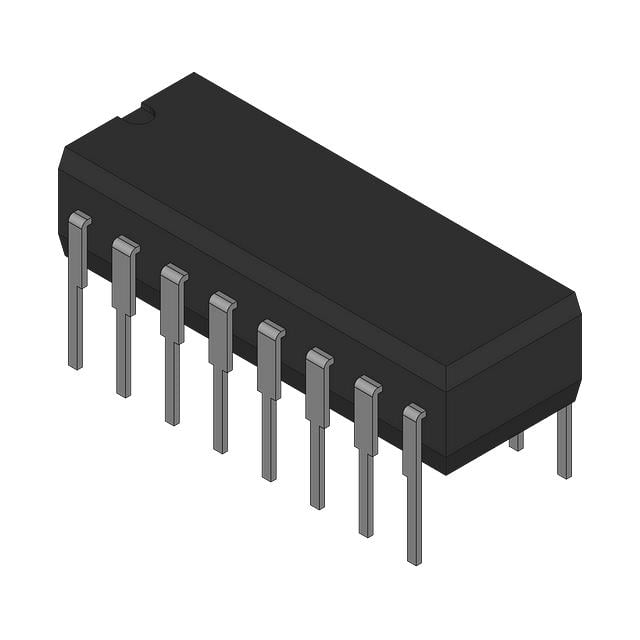
A: The onsemi MC14093BCPG is typically available in a 14-pin plastic dual in-line package (DIP). This package type allows for easy integration into both through-hole and surface-mount designs. The DIP package is commonly used in prototyping and standard circuit board designs, ensuring compatibility with a wide range of systems.
---
Q15: Can the MC14093BCPG be used for clock pulse generation?
A: Yes, the onsemi MC14093BCPG can be used for clock pulse generation in digital circuits. The NAND gates in the device can be configured to create oscillator circuits that generate square wave clock pulses for synchronizing timing in sequential logic systems. The Schmitt trigger inputs help to clean the signal, ensuring stable clock pulses.
---
Q16: What is the output drive capability of the onsemi MC14093BCPG?
A: The MC14093BCPG has typical output drive capabilities that are compatible with CMOS-level logic. It can drive standard CMOS inputs and provide sufficient current to interface with other logic devices. The exact drive capability will depend on the supply voltage and load conditions, but typically, it can source and sink current in the range of 4mA to 8mA.
---
Q17: Can the MC14093BCPG operate at temperatures outside the standard range?
A: The onsemi MC14093BCPG is rated for operation in the standard temperature range of -40°C to +85°C. For applications requiring operation in harsher environments, such as industrial or automotive applications, it is important to select a device that is rated for extended temperature ranges. Operating the device outside of its specified range may lead to unreliable performance.
---
Q18: How does the MC14093BCPG perform in high-frequency applications?
A: The MC14093BCPG is suitable for high-frequency applications, as it offers fast switching speeds, with typical propagation delays around 50ns. This makes it effective for logic operations in high-speed digital circuits, such as clock signals, communication systems, or signal conditioning in fast processing systems.
---
Q19: Does the onsemi MC14093BCPG support both logic high and low inputs?
A: Yes, the MC14093BCPG supports both logic high and low inputs. The Schmitt trigger inputs ensure that even with slow or noisy input transitions, the logic levels are properly recognized and filtered. The device recognizes logic levels according to the supply voltage (Vcc) and operates in a reliable manner with clean transitions.
---
Q20: How can the MC14093BCPG improve signal integrity in digital circuits?
A: The onsemi MC14093BCPG improves signal integrity by using Schmitt trigger inputs that offer noise filtering and better transition handling. These inputs ensure that signals with slow rise times or noise are properly cleaned, which is especially important in systems with high-speed digital communication or where stable logic transitions are critical. The device helps to eliminate false triggering and improves the overall reliability of the digital circuit.