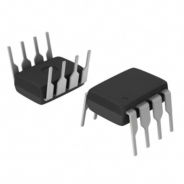
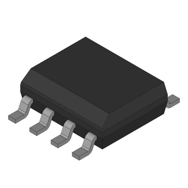
The STMicroelectronics LM201AN is a precision operational amplifier based on a bipolar transistor input architecture, designed for high-gain analog signal processing applications requiring stable DC accuracy, predictable frequency response, and robust closed-loop behavior. It belongs to the LM201 family of general-purpose precision op-amps widely used in instrumentation, industrial control, and analog computation circuits where accuracy and stability are more critical than ultra-low power consumption or rail-to-rail operation.
## Device classification and functional positioning
The LM201AN is a single operational amplifier implemented using a monolithic bipolar junction transistor (BJT) process. It functions as a high-gain differential amplifier with internal frequency compensation, enabling stable operation across a wide range of closed-loop configurations without external compensation components.
The device is positioned within precision analog amplifier ICs intended for linear signal conditioning. It supports standard op-amp configurations including inverting amplification, non-inverting amplification, voltage followers, active filtering, integration, and differentiation functions.
The “AN” suffix indicates a dual in-line package (DIP) variant, typically used for through-hole PCB assembly and prototyping environments where mechanical robustness and ease of handling are required.
## Electrical characteristics and key parameters
The LM201AN operates from dual supply rails or single supply configurations within specified voltage limits defined by internal transistor breakdown and safe operating area constraints. The device is designed for linear operation within a defined input common-mode and output swing range.
Key electrical parameters include input offset voltage, which defines the differential input voltage required to force the output to zero under closed-loop unity gain conditions. This parameter is critical for DC precision applications.
Input bias current is determined by the base current of the input differential transistor pair. This current introduces error when interfacing with high-impedance signal sources and must be accounted for in precision analog design.
Open-loop gain is high, enabling accurate closed-loop gain setting through external feedback networks. The gain is frequency-dependent and decreases as frequency increases due to internal compensation.
The device exhibits a defined gain-bandwidth product, which governs the trade-off between closed-loop gain and usable bandwidth in signal amplification applications.
## Internal architecture and compensation mechanism
The LM201AN is built around a bipolar differential input stage, a high-gain intermediate amplification stage, and a push-pull output stage. The differential input stage provides high transconductance and good common-mode rejection performance.
Internal frequency compensation is implemented using a dominant pole technique. This ensures unity-gain stability by introducing a controlled roll-off in open-loop gain at low frequency, preventing oscillation in standard feedback configurations.
The compensation network defines the slew rate and transient response behavior of the amplifier. The device is optimized for stable operation rather than high-speed performance, prioritizing accuracy and predictable phase margin.
## Input stage characteristics and signal behavior
The input stage uses a matched bipolar transistor pair operating in differential mode. This architecture provides high gain and good DC precision but limits input common-mode voltage range relative to supply rails.
Common-mode rejection ratio (CMRR) is a key performance parameter, indicating the amplifier’s ability to reject signals common to both inputs. This is particularly important in sensor signal conditioning applications where noise and interference are present.
Input offset voltage drift over temperature is determined by transistor matching and thermal gradients across the silicon die.
## Output stage characteristics
The output stage is typically implemented as a class AB push-pull configuration, capable of sourcing and sinking moderate output current into external loads.
Output voltage swing is limited by saturation voltages of the output transistors and does not extend to the supply rails. This is characteristic of non-rail-to-rail bipolar op-amp architectures.
Short-circuit protection may be included to limit output current under fault conditions, protecting the output transistors from thermal overstress.
Output impedance is low under closed-loop operation due to high loop gain, enabling accurate voltage drive capability for external loads.
## Frequency response and dynamic performance
The LM201AN is internally compensated for unity-gain stability, meaning it can be configured as a voltage follower without external compensation components.
The gain-bandwidth product defines the relationship between closed-loop gain and achievable bandwidth. As closed-loop gain increases, usable bandwidth decreases proportionally.
Slew rate defines the maximum rate of change of output voltage and is limited by internal current charging of compensation capacitors. This parameter determines large-signal transient response behavior.
Phase margin is designed to ensure stable operation across standard feedback configurations, preventing oscillation and excessive overshoot in closed-loop circuits.
## Noise performance and precision behavior
The device exhibits low-frequency voltage noise characteristics typical of bipolar input operational amplifiers. Input voltage noise density is determined by base resistance and transistor shot noise mechanisms.
1/f noise contributes to low-frequency noise performance and is relevant in DC and low-frequency measurement systems.
Input bias current noise becomes significant in high-source-impedance applications and contributes to total input-referred noise.
## Power supply and operating conditions
The LM201AN operates from dual or single supply configurations within specified voltage limits. Supply current is relatively constant and defined by internal bias networks of the differential and gain stages.
Power supply rejection ratio (PSRR) defines the ability of the amplifier to suppress variations in supply voltage from appearing at the output. This is important in systems with noisy or unregulated power rails.
Proper decoupling capacitors are required to ensure stability and minimize high-frequency oscillations caused by parasitic inductance in supply routing.
## Package and mechanical configuration
The LM201AN is supplied in a dual in-line package (DIP), typically used for through-hole PCB mounting. This package provides mechanical robustness and ease of prototyping, as well as adequate thermal dissipation for moderate power operation.
The pin configuration includes differential inputs, output terminal, and power supply pins. Internal bonding and lead frame design ensure stable electrical performance under mechanical and thermal stress.
## Application domains
The LM201AN is used in precision analog signal processing systems requiring stable gain, predictable DC behavior, and robust closed-loop performance. Typical applications include:
Instrumentation amplifiers and sensor signal conditioning circuits.
Active filters and analog signal processing networks.
Analog computation circuits including integrators and differentiators.
Industrial control systems requiring stable feedback amplification.
General-purpose precision amplification in measurement equipment.
## Conclusion
The STMicroelectronics LM201AN is a bipolar precision operational amplifier designed for stable DC and low-frequency analog signal processing. Its internal architecture provides high open-loop gain, internal frequency compensation, and predictable closed-loop behavior, making it suitable for instrumentation, industrial control, and analog computation systems where accuracy and stability are primary design requirements.