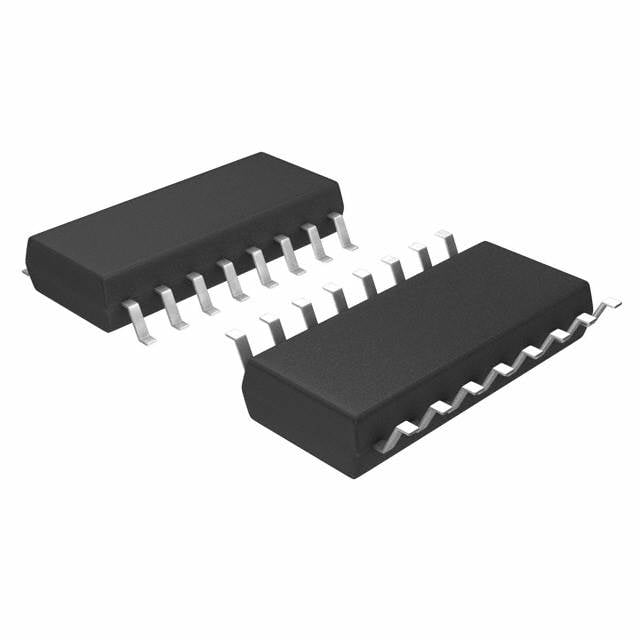
The Texas Instruments CD4066BE is a quad bilateral switch that is widely used in various electronic applications for signal routing and switching. This device is part of the CD4000 series of CMOS (Complementary Metal-Oxide-Semiconductor) logic devices, which are known for their low power consumption and high noise immunity. Below is a detailed introduction to the CD4066BE, including its specifications and typical applications.
## Overview
The CD4066BE consists of four independent switches that can be used to control analog or digital signals. Each switch is bidirectional, meaning that it can pass signals in both directions. This feature makes the CD4066BE versatile for applications such as audio signal routing, data multiplexing, and analog signal processing.
## Key Features
1. Quad Bilateral Switch: The device contains four independent switches, allowing for multiple signal paths to be controlled simultaneously.
2. Low On-Resistance: The on-resistance (R_on) of the switches is low, typically around 50 ohms, which minimizes signal distortion and loss.
3. Wide Supply Voltage Range: The CD4066BE operates over a wide supply voltage range from 3V to 15V, making it suitable for various applications.
4. High Noise Immunity: The CMOS technology used in the CD4066BE provides high noise immunity, ensuring reliable operation in noisy environments.
5. Low Power Consumption: The device consumes very little power, making it ideal for battery-operated devices.
6. High Speed: The switching speed is fast, allowing for quick signal routing without significant delay.
## Specifications
- Supply Voltage (V_DD): 3V to 15V
- Input Voltage Range (V_IN): 0V to V_DD
- On-Resistance (R_on): Typically 50 ohms at V_DD = 9V
- Maximum Continuous Current (I_O): ±10 mA
- Maximum Power Dissipation (P_D): 500 mW
- Operating Temperature Range: -55°C to +125°C
- Propagation Delay: Typically 10 ns
- Control Voltage (V_CTL): 0V to V_DD
## Pin Configuration
The CD4066BE is available in a 14-pin DIP (Dual In-line Package) or SOIC (Small Outline Integrated Circuit) package. The pin configuration is as follows:
- Pin 1: Switch 1 Control (C1)
- Pin 2: Switch 1 Input/Output (A1)
- Pin 3: Switch 1 Input/Output (B1)
- Pin 4: Switch 2 Control (C2)
- Pin 5: Switch 2 Input/Output (A2)
- Pin 6: Switch 2 Input/Output (B2)
- Pin 7: Ground (GND)
- Pin 8: Switch 3 Control (C3)
- Pin 9: Switch 3 Input/Output (A3)
- Pin 10: Switch 3 Input/Output (B3)
- Pin 11: Switch 4 Control (C4)
- Pin 12: Switch 4 Input/Output (A4)
- Pin 13: Switch 4 Input/Output (B4)
- Pin 14: V_DD (Supply Voltage)
## Applications
The CD4066BE is used in a variety of applications, including:
- Audio Signal Switching: It can be used to route audio signals in mixers and effects units.
- Data Multiplexing: The device can switch between multiple data sources in communication systems.
- Analog Signal Processing: It is suitable for applications that require the manipulation of analog signals, such as in filters and modulators.
- Test Equipment: The CD4066BE is often used in test and measurement equipment for signal routing.
## Conclusion
The Texas Instruments CD4066BE is a versatile and reliable quad bilateral switch that offers low on-resistance, wide supply voltage range, and low power consumption. Its ability to handle both analog and digital signals makes it a popular choice in various electronic applications. Whether used in audio processing, data multiplexing, or signal routing, the CD4066BE provides an effective solution for engineers and designers looking to implement switching functions in their circuits.