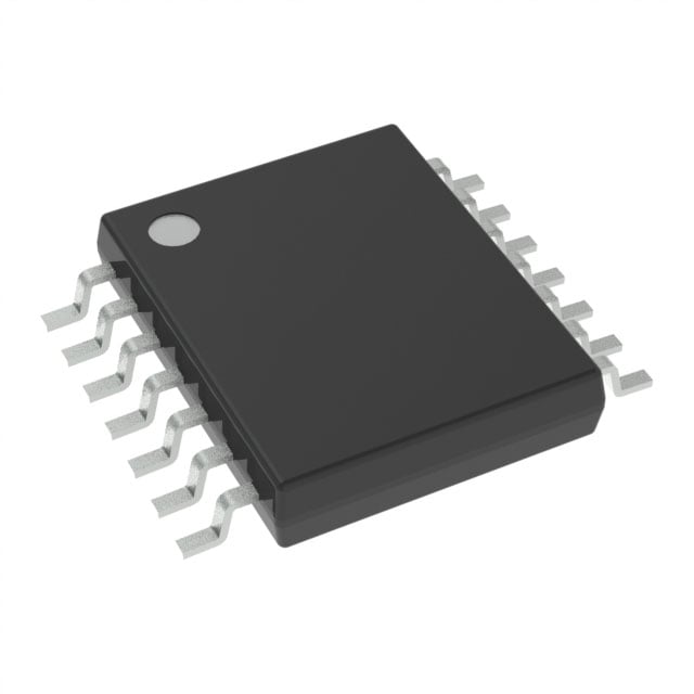
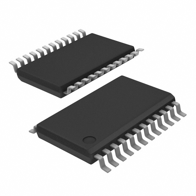
Texas Instruments CDCE913PW Overview
The Texas Instruments CDCE913PW is a versatile, high-performance programmable clock generator designed to provide precise clock frequencies for a wide range of applications, including telecommunications, data communications, and high-speed digital systems. With its advanced features, including programmable outputs, high frequency stability, and low jitter performance, the CDCE913PW is ideal for use in systems that require accurate and flexible clock signal generation.
Key Features
* Programmable Output Frequencies: The CDCE913PW allows for the generation of a wide range of output frequencies, all configurable through a simple I2C interface. This provides flexibility in applications that require different clock speeds for various components.
* Low Jitter Performance: The clock generator offers low jitter characteristics, which are critical for high-speed communication systems where timing accuracy is essential to maintain data integrity and minimize errors.
* Multiple Output Options: It provides multiple output pins (up to 4), each capable of delivering different clock signals, making it an ideal choice for applications requiring multiple synchronized clocks.
* Wide Input Frequency Range: The input frequency range is wide, supporting clock inputs from 10 MHz to 60 MHz, allowing for flexible input source configurations.
* I2C Programmability: The CDCE913PW is programmed through an I2C interface, enabling easy integration into systems with microcontrollers or other I2C-compatible devices. The device configuration can be changed dynamically or during system initialization.
* Low Power Consumption: The IC is designed for low power operation, making it suitable for battery-operated devices or power-sensitive applications.
* Flexible Output Voltage Options: The device supports both 3.3V and 5V output voltage levels, providing compatibility with a wide range of digital logic families.
Electrical Characteristics
* Operating Voltage: The CDCE913PW operates with a supply voltage range of 3.3V to 5V, offering flexibility in both lower voltage and standard 5V systems.
* Input Frequency Range: The IC accepts an input frequency range from 10 MHz to 60 MHz, allowing it to be used in a variety of applications requiring different input clock sources.
* Output Frequency Range: The device can output clock frequencies ranging from 1 MHz to 100 MHz, depending on the input frequency and configuration. The output is adjustable in increments of 1 MHz, providing fine-grained control over the generated clock.
* Clock Output Rise/Fall Time: The rise and fall time of the clock outputs is typically 2.5 ns, which ensures fast signal transitions for high-speed applications.
* Jitter Performance: The CDCE913PW offers a low RMS jitter of less than 20 ps (typical), ensuring stable and reliable clock signals for high-speed and high-precision systems.
* I2C Communication Speed: The I2C interface supports standard mode (100 kHz) and fast mode (400 kHz), ensuring that the device can be programmed efficiently without affecting overall system performance.
Thermal and Mechanical Properties
* Operating Temperature Range: The CDCE913PW is specified to operate within a wide temperature range of -40°C to +85°C, making it suitable for industrial and automotive applications where environmental conditions can vary.
* Thermal Resistance (RθJA): The device has a typical thermal resistance of 38°C/W, ensuring adequate heat dissipation during operation and preventing overheating in high-performance environments.
* Package Type: The CDCE913PW is available in a 16-pin TSSOP (Thin Shrink Small Outline Package), which offers a compact form factor, making it suitable for space-constrained applications such as portable devices, consumer electronics, and industrial systems.
* Weight: The TSSOP package is lightweight and well-suited for high-density designs where minimizing PCB space and weight is critical.
Applications
* Telecommunications: The CDCE913PW is ideal for telecommunications systems that require precise clock synchronization across multiple channels. Its low jitter and programmable output frequencies make it suitable for use in high-speed data transmission applications such as routers, switches, and base stations.
* Data Communication Systems: In data communication systems, the clock generator ensures accurate timing for high-speed serial data interfaces like Ethernet, PCIe, and USB, where synchronization of data signals is crucial for minimizing data errors.
* Embedded Systems: The IC is also used in embedded systems to generate clock signals for microcontrollers, FPGAs, and other digital components. Its I2C programmability allows it to be easily integrated into complex systems.
* Consumer Electronics: The CDCE913PW can be used in consumer electronics like set-top boxes, televisions, and gaming consoles, where multiple clock frequencies are needed to drive different components simultaneously.
* Test Equipment: The low jitter and flexible output frequencies make the CDCE913PW suitable for use in test and measurement equipment, where precise timing and synchronization of multiple signals are required.
* Automotive Systems: Automotive applications that involve complex sensor networks or communication protocols can benefit from the programmable clock generation capabilities of the CDCE913PW, helping to ensure reliable performance in harsh environments.
Advantages of CDCE913PW
* Precision Clock Generation: With its ability to generate precise, programmable clock frequencies, the CDCE913PW is a valuable tool for systems that require high accuracy and low jitter in their timing signals.
* Multiple Outputs: The ability to generate multiple clock signals from a single device simplifies design and reduces the number of components required in systems with complex timing requirements.
* I2C Programmability: The I2C interface makes the CDCE913PW easy to integrate into existing systems, allowing dynamic reconfiguration and minimizing the need for external components or switches.
* Low Power Operation: The CDCE913PW is designed for low power consumption, making it suitable for battery-powered or energy-efficient systems where power savings are crucial.
* Compact and Flexible Package: The TSSOP package is compact and provides flexibility in design, allowing the device to be used in a variety of applications where board space is limited.
* Wide Frequency Range: The wide input and output frequency ranges, along with fine granularity of frequency adjustment, ensure that the device can be used in diverse applications requiring different clock speeds.
Conclusion
The Texas Instruments CDCE913PW is a highly versatile and efficient programmable clock generator that provides precise clock frequencies for a wide variety of applications. With its low jitter, wide input and output frequency ranges, and I2C programmability, the CDCE913PW is an ideal choice for systems requiring accurate and flexible clock signal generation. Whether used in telecommunications, data communication systems, consumer electronics, or embedded systems, this IC offers significant advantages in terms of performance, integration, and energy efficiency. Its compact package and low power operation make it well-suited for space-constrained and power-sensitive applications, providing reliable performance across a wide range of environments and use cases.