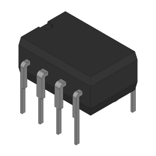
Texas Instruments TLC082CDR Detailed Professional Overview
General Description
The Texas Instruments TLC082CDR is a dual operational amplifier device belonging to the TLC08xx family, designed with JFET input stages. It combines low input bias currents, low input offset voltage, and high slew rates, making it suitable for precision analog signal processing applications. The device features two independent, high-gain, internally frequency-compensated operational amplifiers intended for a wide range of analog circuits including filtering, buffering, and signal conditioning.
Architecture and Technology
The TLC082CDR utilizes JFET input stages that provide extremely low input bias currents (typically in picoamperes), enabling excellent performance in high-impedance sensor interface circuits. The device is manufactured using advanced CMOS technology, allowing it to operate at low supply currents while maintaining high bandwidth and low noise. The internal frequency compensation ensures stable operation without the need for external components across a wide range of gain settings.
Key Features
* Dual operational amplifier in a single 8-pin SOIC package
* Low input bias current: typically 20 pA at 25°C
* Low input offset voltage: typically 3 mV, maximum 7 mV
* High slew rate: typically 5 V/μs
* Wide supply voltage range: ±3 V to ±16 V (or 6 V to 32 V single supply)
* Rail-to-rail output swing capability (within approximately 1.5 V of supply rails)
* High input impedance due to JFET inputs
* Low quiescent supply current: typically 1.4 mA per amplifier
* Wide gain bandwidth product: 3 MHz typical
* Internal frequency compensation for unity-gain stability
* Compatible with single and dual supply operation
* Low total harmonic distortion suitable for audio and precision analog applications
Electrical Specifications
* Supply Voltage (VDD to VSS): 6 V to 32 V (single supply) or ±3 V to ±16 V (dual supply)
* Input Offset Voltage (VOS): Typically 3 mV; maximum 7 mV
* Input Bias Current (IB): Typically 20 pA at 25°C
* Input Offset Current (IOS): Typically 2 pA at 25°C
* Input Voltage Range: Extends to within 3 V of positive supply rail and to negative rail
* Output Voltage Swing: Typically can swing within 1.5 V of rails with 10 kΩ load
* Slew Rate: 5 V/μs typical, ensuring fast response to input changes
* Gain Bandwidth Product (GBP): 3 MHz typical
* Total Harmonic Distortion + Noise (THD+N): 0.003% at 1 kHz, 2 V peak-to-peak output
* Common-Mode Rejection Ratio (CMRR): 70 dB typical
* Power Supply Rejection Ratio (PSRR): 70 dB typical
* Quiescent Current: Approximately 1.4 mA per amplifier at 5 V supply
* Operating Temperature Range: -40°C to +85°C (industrial grade)
Pin Configuration and Package
The TLC082CDR is packaged in an 8-pin SOIC form factor, providing two operational amplifiers with the following typical pin assignments:
* Pins for two inputs (inverting and non-inverting) per amplifier
* Two output pins for each amplifier
* Power supply pins (VDD and VSS)
* Offset null pins are not present, reflecting the internally trimmed offset
Performance and Functional Characteristics
The JFET input stage provides high input impedance and low input bias currents, critical for interfacing with high-impedance sensors or charge amplifiers. The device exhibits low input offset voltage and low noise, contributing to accurate signal amplification with minimal distortion. Its internal compensation ensures stability for gains as low as unity, facilitating buffer configurations.
The output stage can swing close to supply rails but is not rail-to-rail; it typically maintains about 1.5 V margin from each rail under moderate load. This characteristic must be considered when designing single-supply systems, especially at lower supply voltages.
Applications
* High-impedance sensor amplification (e.g., photodiodes, piezoelectric sensors)
* Active filters and integrators
* Voltage followers and buffers
* Audio preamplifiers and signal conditioning
* Medical instrumentation and data acquisition systems
* Precision DC amplification in industrial control systems
* Battery-powered portable devices, benefiting from low supply current
Typical Application Circuits
The TLC082CDR is commonly used in buffer configurations due to its unity-gain stability and low input bias current. It is also well-suited for instrumentation amplifiers when combined with precision resistors. The device can form the active element in low-pass or high-pass filters and oscillators requiring low distortion and stable gain.
Reliability and Environmental Compliance
The device operates reliably over a wide industrial temperature range and meets standard quality and environmental compliance standards. Its robust CMOS construction provides good immunity against latch-up and electrostatic discharge.
Summary
Texas Instruments’ TLC082CDR is a versatile dual operational amplifier featuring JFET inputs that offer high input impedance, low input bias current, and low offset voltage. Its wide supply voltage range, internal frequency compensation, and decent slew rate make it a solid choice for precision analog signal processing tasks in industrial, medical, and portable electronic systems. While it is not a rail-to-rail input/output amplifier, its performance characteristics provide a balance between precision, speed, and power efficiency suitable for a broad range of applications requiring quality amplification with low noise and distortion.