Introduction to Xilinx XC3042A-7VQ100C
The Xilinx XC3042A-7VQ100C is a field-programmable gate array (FPGA) that belongs to the XC3000 series, which is known for its flexibility, performance, and efficiency in digital logic design. This device is particularly favored in applications requiring custom hardware solutions due to its reconfigurability and ability to implement complex digital circuits without the need for custom silicon fabrication.
Key Specifications
1. Device Architecture: The XC3042A utilizes a SRAM-based architecture that allows for reconfiguration and high-speed processing capabilities. This architecture provides designers with the ability to modify their designs post-manufacturing, accommodating changes in requirements or specifications.
2. Logic Cells: The XC3042A-7VQ100C features approximately 4,032 logic cells. Each logic cell consists of a combination of look-up tables (LUTs) and flip-flops, enabling the implementation of various combinational and sequential logic functions.
3. I/O Pins: This FPGA includes 100 I/O pins, offering considerable flexibility for interfacing with other components in a system. The I/O pins support multiple voltage levels and can be configured for different signaling standards.
4. Operating Voltage: The device operates at a supply voltage range of 4.5V to 5.5V, making it compatible with standard TTL (Transistor-Transistor Logic) and CMOS (Complementary Metal-Oxide-Semiconductor) technologies.
5. Speed Grade: The "-7" in the part number indicates that this FPGA has a speed grade of 7, which allows it to operate at maximum clock frequencies up to 50 MHz under typical conditions. This speed is suitable for many real-time processing applications.
6. Configuration Method: The XC3042A supports various configuration methods including JTAG (Joint Test Action Group), which simplifies programming and debugging processes. Additionally, it can be configured using external memory devices or through direct programming.
7. Block RAM: The device comes equipped with embedded block RAM resources that can be utilized for data storage purposes, enhancing its capability to handle larger datasets or buffering requirements within applications.
8. Power Consumption: The XC3042A is designed with power efficiency in mind, typically consuming around 500 mW during active operation depending on the configuration and usage scenario. This characteristic makes it suitable for battery-operated devices as well as other power-sensitive applications.
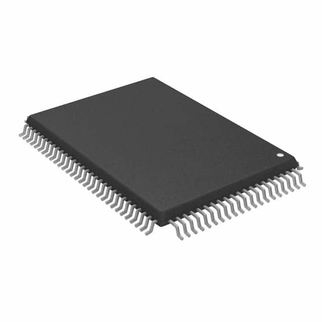
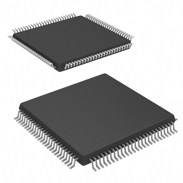
9. Package Type: The XC3042A-7VQ100C is housed in a VQFP (Very Thin Quad Flat Package) package type with 100 pins, allowing for easy integration into printed circuit boards while maintaining a compact footprint.
10. Applications: This FPGA is widely used in various fields such as telecommunications, automotive systems, industrial control systems, consumer electronics, and military applications due to its adaptability and performance characteristics.
Applications
The Xilinx XC3042A-7VQ100C FPGA finds its place in numerous applications including:
- Digital signal processing where custom algorithms need to be implemented efficiently.
- Communication systems that require rapid data handling and protocol management.
- Robotics where real-time processing and control are essential.
- Prototyping of digital circuits where flexibility in design changes is necessary before final production.
Conclusion
In conclusion, the Xilinx XC3042A-7VQ100C represents a powerful solution for engineers seeking an adaptable FPGA capable of meeting diverse application needs. Its combination of ample logic resources, flexible I/O configurations, and efficient power consumption makes it an excellent choice for both prototyping and production environments across various industries. By leveraging this FPGA's capabilities, designers can create innovative solutions tailored to their specific project requirements while benefiting from the advantages of programmable hardware technology.
.jpg)