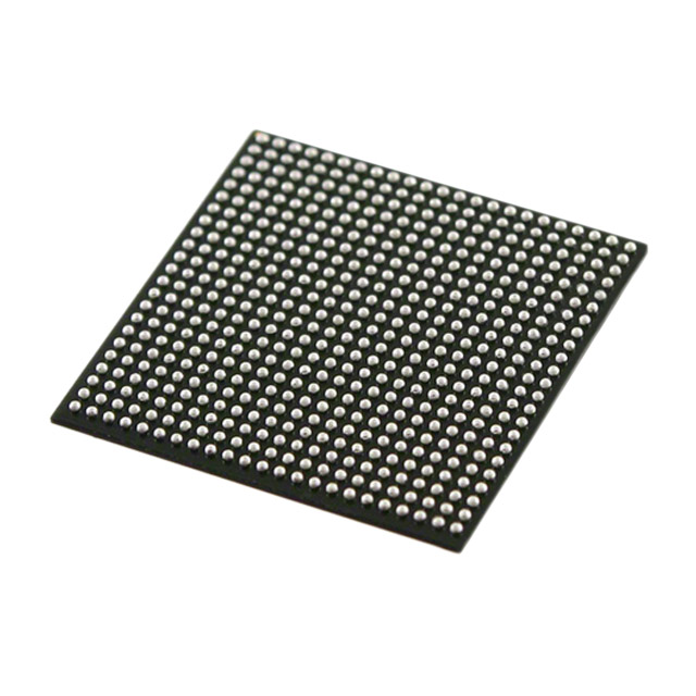
## Overview
The Intel 5CEBA2F23C8N is a member of the Cyclone V FPGA family, designed to deliver low-power, cost-efficient, and high-performance programmable logic solutions for embedded, industrial, and consumer applications. Built on a 28 nm process technology, the device integrates a rich set of programmable logic resources, embedded memory, DSP blocks, and high-speed I/O interfaces, providing a versatile platform for system integration. The Cyclone V family emphasizes low static and dynamic power while enabling complex logic and signal processing functions in a compact footprint.
## Architecture
* Technology: 28 nm low-power FPGA process
* Logic Elements (LEs): 22,320
* Adaptive Logic Modules (ALMs): 6,720
* Configurable Logic Blocks (CLBs): Each ALM contains 2 LUTs and 4 registers, supporting flexible combinational and sequential logic
* Embedded Memory: 594 Kbits of MLAB and 2,112 Kbits of embedded M20K block RAM
* DSP Blocks: 80 18×18-bit multipliers for high-performance arithmetic and signal processing
* Phase-Locked Loops (PLLs): 12 dedicated PLLs for clock management, frequency synthesis, and deskewing
* I/O Pins: 230
* Package: 230-pin FBGA
* Speed Grade: 8 (commercial range)
* Operating Temperature: 0°C to +85°C
* Supports both synchronous and asynchronous logic with deterministic timing
* Integrated hard memory controllers for DDR3 and other external memory interfaces
The Cyclone V architecture combines high-density logic, embedded memory, DSP capabilities, and flexible I/O in a single low-power FPGA for industrial and embedded applications.
## Logic Resources
* Total Logic Elements: 22,320
* ALMs: 6,720, each containing 2 adaptive LUTs and 4 flip-flops
* Flip-Flops: Embedded for sequential logic across ALMs
* Look-Up Tables (LUTs): 6-input LUTs per ALM, supporting complex combinational functions
* Maximum User-Defined Functions: Determined by ALM and LUT configuration
* DSP Capabilities: 80 embedded 18×18 multipliers with optional accumulation for arithmetic, filtering, and digital signal processing
* Embedded Memory: 594 Kbits distributed RAM (MLAB) and 2,112 Kbits block RAM (M20K)
* Supports implementation of finite-state machines, arithmetic functions, data buffering, and signal processing pipelines
* Deterministic timing ensures predictable operation across multiple clock domains
## I/O Features
* Total I/O Pins: 230
* Supported I/O Standards: LVCMOS, LVTTL, SSTL, HSTL, LVDS, and PCIe-compatible differential signaling
* Input Thresholds: Configurable per I/O bank
* Output Drive: Programmable drive strength and slew rate
* Pin-to-Pin Propagation Delay: 1–3 ns typical depending on path and configuration
* I/O Banks: Segmented to support multiple voltage standards for heterogeneous system integration
* Flexible I/O configuration allows interfacing with microcontrollers, memory, high-speed transceivers, ADC/DACs, and sensors
## Timing Characteristics
* Maximum System Clock Frequency: Up to 400 MHz for general logic paths depending on design constraints
* Maximum DSP Clock Frequency: 600 MHz for embedded DSP blocks
* Embedded Memory Maximum Clock Frequency: 400 MHz
* Pin-to-Pin Propagation Delay: 1–3 ns typical depending on interconnect and load
* Supports multi-clock domain designs with integrated PLLs, global clock networks, and dedicated clock routing resources
* Deterministic timing suitable for real-time control, signal processing, and interface bridging
## Power Characteristics
* Core Voltage (VCCINT): 1.0 V typical
* I/O Voltage (VCCIO): 1.2 V, 1.8 V, 2.5 V, or 3.3 V depending on bank configuration
* Typical Power Consumption: 1–2 W under moderate utilization
* Maximum Power Consumption: Approximately 4 W under full utilization
* Low static and dynamic power consumption achieved through 28 nm process and Cyclone V low-power architecture
* Supports power-down and partial reconfiguration modes for energy-efficient system design
## Package and Integration
* Package: 230-pin FBGA with 0.8 mm ball pitch
* High pin count and high-density logic suitable for compact industrial and embedded PCB layouts
* Integrated M20K RAM, DSP blocks, and hard memory controllers reduce external component count
* Multi-voltage I/O banks enable flexible interfacing with heterogeneous systems
* High integration allows complex digital signal processing, control, and interface functions in a single FPGA
## Applications
* Industrial automation and embedded control systems
* Digital signal processing and interface bridging
* Consumer electronics requiring low power and compact footprint
* Communication protocol interfacing and high-speed peripheral connectivity
* Finite-state machine implementation, arithmetic logic, buffering, and signal processing pipelines
## Development and Tool Support
* Supported by Intel Quartus Prime software for design entry, synthesis, placement, routing, timing analysis, simulation, and device programming
* JTAG interface available for in-system programming, boundary-scan testing, and debugging
* IP cores for memory controllers, DSP functions, high-speed interfaces, and communication protocols accelerate system design
* Timing analysis, simulation, and power estimation tools enable verification of multi-clock domain, high-speed, and signal-intensive applications
* Flash-based or SRAM-based configuration options provide instant-on operation and reliable deployment in industrial and consumer environments
The Intel 5CEBA2F23C8N Cyclone V FPGA offers a high-density, low-power platform with integrated logic, memory, DSP blocks, and flexible I/O. Its 28 nm architecture, deterministic timing, and multi-clock support make it suitable for embedded, industrial, and consumer applications that demand performance, integration, and energy efficiency.