The Texas Instruments ADC128S102CIMTX is an 8-channel, 12-bit successive approximation register (SAR) analog-to-digital converter (ADC) designed for low-power, high-speed data acquisition in a compact form factor. It is optimized for applications requiring multiple analog input channels, such as medical imaging, industrial automation, and sensor interfacing. The device is housed in a 16-pin TSSOP package and is supplied in tape-and-reel format, making it suitable for high-volume manufacturing. Below is a comprehensive exploration of the ADC128S102CIMTX, covering its features, specifications, functionality, and applications, organized under relevant subheadings.
Overview
The ADC128S102CIMTX is a versatile ADC that integrates eight single-ended analog input channels, a high-speed SAR architecture, and an SPI-compatible serial interface. It is designed to provide accurate and efficient conversion of analog signals to digital data with minimal power consumption, making it ideal for battery-powered and space-constrained applications. The device operates over a wide supply voltage range and includes on-chip sample-and-hold circuitry, eliminating the need for external components in many designs. Its high-speed conversion rate and multi-channel capability make it suitable for applications requiring simultaneous sampling of multiple analog signals.
Key Features
The ADC128S102CIMTX offers a robust set of features tailored for precision data acquisition:
- 8-Channel Multiplexed Inputs: Supports eight single-ended analog input channels, enabling simultaneous monitoring of multiple signals.
- 12-Bit Resolution: Provides high-precision conversion with 12-bit resolution for accurate digital representation of analog inputs.
- High-Speed Conversion: Offers a sampling rate of up to 1 MSPS (megasamples per second), suitable for real-time applications.
- Low Power Consumption: Consumes as low as 1.2 mW at 3 V and 7.5 mW at 5 V during normal operation, with a power-down mode reducing consumption to 2.3 µW.
- SPI-Compatible Interface: Features a serial peripheral interface (SPI) for easy integration with microcontrollers and DSPs, supporting standards like QSPI and MICROWIRE.
- Internal Voltage Reference: Uses the supply voltage as the reference, simplifying system design by eliminating the need for an external reference.
- On-Chip Sample-and-Hold: Includes integrated sample-and-hold circuitry for accurate signal capture without external components.
- Wide Supply Voltage Range: Operates from 2.7 V to 5.25 V for both analog and digital supplies, offering flexibility for various power domains.
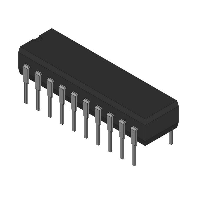
- Compact Package: Housed in a 16-pin TSSOP package, ideal for space-constrained designs.
- Lead-Free and RoHS Compliant: Environmentally friendly with a Moisture Sensitivity Level (MSL) of 1 (unlimited).
Specifications
The following are the key technical specifications of the ADC128S102CIMTX:
- Resolution: 12 bits.
- Number of Channels: 8 single-ended analog input channels.
- Sampling Rate: 50 kSPS to 1 MSPS (adjustable).
- Supply Voltage:
- Analog Supply: 2.7 V to 5.25 V.
- Digital Supply: 2.7 V to 5.25 V.
- Power Consumption:
- Normal Operation: 1.2 mW at 3 V, 7.5 mW at 5 V (at 200 kSPS).
- Power-Down Mode: 2.3 µW at 5 V.
- Integral Nonlinearity (INL): ±1 LSB (least significant bit).
- Differential Nonlinearity (DNL): ±0.8 LSB.
- Signal-to-Noise Ratio (SNR): 73 dB typical.
- Total Harmonic Distortion (THD): -83 dB typical.
- Input Voltage Range: 0 V to VREF (supply voltage).
- Reference Voltage: Supply voltage (2.7 V to 5.25 V).
- Data Interface: SPI, QSPI, MICROWIRE, DSP-compatible serial interface.
- Package: 16-pin TSSOP (4.4 mm width).
- Operating Temperature Range: -40°C to +105°C.
- Conversion Time: Approximately 1 µs per channel at maximum sampling rate.
- Input Impedance: High input impedance for minimal loading of analog sources.
- ESD Protection: Robust ESD protection for reliable operation in various environments.
Functional Description
The ADC128S102CIMTX operates using a successive approximation register (SAR) architecture, which provides a balance of speed, accuracy, and power efficiency. The device features eight single-ended analog input channels, which are multiplexed into a single ADC core. The integrated sample-and-hold circuit captures the analog input signal during the sampling phase, ensuring accurate conversion without external circuitry. The conversion process is initiated via the SPI interface, where the user can select the active channel and configure the sampling rate.
The device outputs 12-bit digital data in a straight binary format, compatible with various serial communication standards. The SPI interface supports clock frequencies up to 16 MHz, enabling fast data transfer. The internal voltage reference is tied to the supply voltage, simplifying system design but requiring a stable power supply for optimal performance. The power-down mode, activated via the SPI interface, significantly reduces power consumption during idle periods, making the device suitable for battery-operated systems.
Applications
The ADC128S102CIMTX is well-suited for a wide range of applications, including:
- Medical Imaging: Used in MRI and CT scanners for digitizing analog signals from sensors, leveraging its multi-channel capability and high resolution.
- Industrial Automation: Monitors multiple sensor inputs (e.g., temperature, pressure, or voltage) in real-time for process control and data logging.
- Portable Instrumentation: Its low power consumption and compact size make it ideal for handheld devices like multimeters and data loggers.
- Motor Control: Provides precise analog-to-digital conversion for feedback signals in motor control systems.
- Data Acquisition Systems: Supports multi-channel data acquisition in systems requiring high-speed, accurate signal conversion.
- Consumer Electronics: Used in devices like fitness trackers or smart home sensors for analog signal processing.
Design Considerations
When integrating the ADC128S102CIMTX into a system, designers should consider the following:
- Power Supply Stability: Since the supply voltage serves as the reference, a stable and low-noise power supply is critical for maintaining conversion accuracy.
- PCB Layout: Careful layout is required to minimize noise coupling into the analog inputs. Separate analog and digital ground planes are recommended, with proper decoupling capacitors near the supply pins.
- Input Signal Conditioning: External anti-aliasing filters may be needed depending on the input signal frequency to prevent aliasing artifacts.
- SPI Interface: The microcontroller or DSP interfacing with the ADC must support SPI, QSPI, or MICROWIRE protocols and handle clock frequencies up to 16 MHz.
- Channel Selection: The multiplexer allows sequential or random channel selection via the SPI interface, requiring proper configuration in software.
- Thermal Management: The device operates reliably up to 105°C, but thermal considerations are important in compact or high-temperature environments.
Advantages
The ADC128S102CIMTX offers several advantages for system designers:
- Multi-Channel Flexibility: Eight input channels allow monitoring of multiple signals without additional ADCs, reducing system cost and complexity.
- Low Power Efficiency: Its low power consumption is ideal for battery-powered applications, extending operational life.
- Compact Design: The 16-pin TSSOP package saves board space, making it suitable for space-constrained designs.
- Ease of Integration: The SPI-compatible interface and internal reference simplify system design and reduce external component count.
- Wide Operating Range: The broad supply voltage and temperature range enhance its versatility across applications.
Limitations
Despite its strengths, the ADC128S102CIMTX has some limitations:
- Single-Ended Inputs Only: The device does not support differential inputs, which may limit its use in applications requiring high common-mode rejection.
- No Internal Reference Option: The lack of a dedicated internal reference voltage may require additional care in power supply design for high-accuracy applications.
- Limited Resolution: While 12-bit resolution is sufficient for many applications, higher-resolution ADCs (e.g., 16-bit or 18-bit) may be needed for ultra-precise measurements.
- Sequential Conversion: The single ADC core means channels are converted sequentially, which may introduce slight delays in multi-channel applications compared to simultaneous-sampling ADCs.
Comparison with Related Devices
The ADC128S102CIMTX is part of Texas Instruments’ ADC128S series, with variants like the ADC128S052 (same specifications but different packaging options) and ADC128S022 (lower sampling rate). Compared to the Analog Devices ADAS1000BSTZ-RL (a 5-channel, 19-bit ECG-specific AFE), the ADC128S102CIMTX is more general-purpose, with lower resolution but higher channel count and broader application scope. Against competitors like the Analog Devices AD7944 (14-bit, 2.5 MSPS) or Microchip’s MCP3208 (8-channel, 10-bit), the ADC128S102CIMTX offers a balanced combination of resolution, speed, and power efficiency, though it may not match the sampling rate of higher-end ADCs.
Conclusion
The Texas Instruments ADC128S102CIMTX is a highly capable, low-power, 8-channel, 12-bit SAR ADC that excels in applications requiring multi-channel analog-to-digital conversion. Its high-speed sampling, compact TSSOP package, and SPI-compatible interface make it a versatile choice for medical, industrial, and portable applications. While it lacks differential inputs and a dedicated internal reference, its integration, power efficiency, and flexibility make it a strong contender for cost-sensitive, space-constrained designs. Engineers seeking a reliable, multi-channel ADC for real-time signal processing will find the ADC128S102CIMTX an excellent solution, supported by its robust performance and ease of integration.