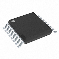
Overview of onsemi TL494BDR2G
The onsemi TL494BDR2G is a versatile integrated circuit primarily used for pulse width modulation (PWM) control in power supplies and DC-DC converters. This device is designed to facilitate efficient power management, enabling users to implement various control strategies in switching power supplies. The TL494BDR2G combines multiple functions within a single chip, making it an ideal choice for applications that require precise voltage regulation and high efficiency.
Key Specifications
- Supply Voltage Range: The TL494BDR2G operates with a supply voltage range of 7V to 40V, which allows for flexibility in various power supply designs.
- Output Frequency: The oscillator frequency can be adjusted from 100 Hz to 100 kHz, providing versatility for different applications and load requirements.
- Output Drive Capability: The device features a totem-pole output stage that can source or sink up to 200 mA, making it suitable for driving external transistors or MOSFETs directly.
- Dead Time Control: The TL494BDR2G includes adjustable dead time control, allowing designers to fine-tune the switching characteristics of the converter, which helps minimize cross-conduction losses.
- Error Amplifier: It incorporates two error amplifiers with a high gain bandwidth product, enabling precise feedback control for voltage regulation.
- Temperature Range: The operating temperature range is from -40°C to +85°C, ensuring reliable performance in various environmental conditions.
Functional Features
The TL494BDR2G integrates several functional features that enhance its performance and usability:
- PWM Control: The primary function of the TL494BDR2G is to provide PWM control for switch-mode power supplies. This allows for efficient energy conversion and regulation.
- Voltage Regulation: The device supports both voltage mode and current mode control strategies, providing flexibility in design approaches depending on application requirements.
- Dual Outputs: It offers two outputs (OUT1 and OUT2), which can be configured for push-pull operation or used independently to drive different components in a power supply circuit.
- Soft Start Feature: The soft start functionality helps limit inrush current during startup, preventing damage to components and improving reliability.
Applications
The TL494BDR2G is widely utilized across various applications due to its robust design and extensive functionality:
- Switching Power Supplies: Commonly used in AC-to-DC converters and DC-to-DC converters where efficient voltage regulation is required.
- Battery Chargers: Suitable for use in battery charging circuits where precise control over charging currents and voltages is necessary.
- Industrial Power Supplies: Employed in industrial equipment requiring reliable power management solutions with adjustable output characteristics.
- Consumer Electronics: Used in consumer electronics such as televisions, computers, and audio systems where efficient power conversion is essential.
Pin Configuration
The TL494BDR2G comes in a 16-pin surface-mount package (SOIC), with the following pin configuration:
1. Compensation (1): Connects to compensation network for stability of the error amplifier.
2. Error Amplifier Inverting Input (2): Inverting input of the error amplifier; connects to feedback from the output voltage.
3. Error Amplifier Non-Inverting Input (3): Non-inverting input of the error amplifier; typically connected to a reference voltage.
4. Output 1 (4): First PWM output; drives external switching devices like transistors or MOSFETs.
5. Output 2 (5): Second PWM output; can be used independently or configured for push-pull operation with Output 1.
6. Dead Time Adjustment (6): Pin used to set the dead time between outputs; connects to an external resistor-capacitor network for adjustment.
7. Oscillator Timing Capacitor (7): Connects timing capacitor for oscillator frequency adjustment; sets the frequency of PWM signal generation.
8. Ground (8): Common ground connection for proper operation of the IC.
9. VCC (9): Supply voltage input; powers the internal circuitry of the IC.
10. Voltage Reference Output (10): Provides a stable reference voltage output typically at 5V; can be used in feedback loops or other circuit functions.
11. Current Limit Setting (11): Pin used to set current limit thresholds; connects to external resistors or components as needed.
12. Shutdown Control (12): Allows external shutdown control by pulling this pin low; disables outputs when not needed.
13. Feedback Input (13): Feedback pin that connects back from the output voltage sensing point; provides feedback signal for regulation purposes.
14. Sync Input/Output (14): Pin used for synchronization with other devices if required; can help coordinate multiple PWM controllers.
15. Soft Start Control (15): Connects soft-start capacitor/resistor network; limits initial current during startup phase.
16. Oscillator Timing Resistor (16): Connects timing resistor for setting oscillator frequency along with timing capacitor.
Conclusion
In summary, the onsemi TL494BDR2G is a highly versatile PWM controller designed for efficient power management across various applications, including switching power supplies and battery chargers. Its comprehensive specifications, including adjustable frequency, dual outputs, and integrated error amplifiers, make it an ideal choice for engineers looking to implement reliable and efficient power solutions. With its robust performance over a wide temperature range and flexible design capabilities, the TL494BDR2G continues to be a popular choice in modern electronic designs.