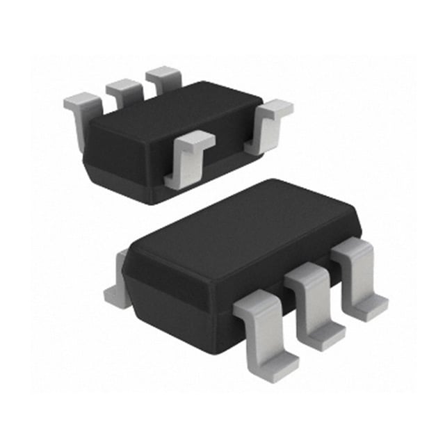
STMicroelectronics TS1871AIDT is a low-power rail-to-rail operational amplifier designed for general-purpose analog signal conditioning in single-supply systems. It is optimized for low-voltage operation, low quiescent current consumption, and stable performance across a wide range of industrial and portable applications. The device provides a combination of low offset voltage, low noise, and rail-to-rail input/output capability, making it suitable for battery-powered systems and precision signal processing circuits.
## Device Function and Product Positioning
The TS1871AIDT belongs to STMicroelectronics’ TS187x family of low-power operational amplifiers. Its primary function is to amplify, buffer, and condition analog signals in single-supply or low-voltage environments.
The device is designed for applications where both input and output signal swing must extend close to the supply rails, enabling maximum dynamic range in low-voltage systems such as 3.3 V and 5 V electronics.
The “AIDT” suffix indicates a specific package and qualification variant, typically associated with SO-8 surface-mount packaging and industrial temperature-grade operation.
The amplifier is intended for cost-sensitive, power-efficient analog signal processing rather than high-speed or high-current drive applications.
## Electrical Supply Characteristics and Operating Conditions
The TS1871AIDT operates from a single supply or dual supply configuration depending on system design requirements. It is optimized for low-voltage operation, supporting modern embedded systems and portable electronics.
The supply current is characterized as low quiescent current per amplifier, making it suitable for always-on analog front-end circuits where power consumption must be minimized.
The device maintains stable operation across its full recommended supply range, with internal biasing designed to ensure consistent performance even under supply variation.
## Input Stage Architecture and Rail-to-Rail Operation
A key feature of the TS1871AIDT is its rail-to-rail input stage. This architecture allows the common-mode input voltage range to extend close to both the negative and positive supply rails.
This is achieved through a complementary differential input pair structure, ensuring continuous transconductance across the full input voltage range.
The rail-to-rail input capability is particularly important in low-voltage systems where signal levels may approach supply boundaries, such as sensor outputs in battery-powered devices.
## Output Stage Characteristics
The output stage of the TS1871AIDT is also rail-to-rail capable, allowing the output voltage to swing close to both supply rails under light load conditions.
The output stage is typically designed using a class AB push-pull configuration, optimized for low static power consumption and moderate load driving capability.
Output voltage swing is dependent on load resistance and supply voltage conditions, with performance optimized for high impedance loads and moderate capacitive loading.
## Key Electrical Parameters (datasheet-level characteristics)
The TS1871AIDT is characterized by several precision analog parameters:
Low input offset voltage, enabling accurate DC signal amplification
Low input bias current, suitable for high impedance sensor interfaces
Low supply current per amplifier, supporting battery-powered operation
Gain bandwidth product suitable for low-frequency to mid-frequency signal conditioning
Slew rate optimized for stability rather than high-speed switching
High input common-mode rejection ratio (CMRR)
High power supply rejection ratio (PSRR)
These parameters are defined under controlled test conditions and are intended for precision low-frequency analog applications rather than RF or high-speed signal processing.
## Noise Performance and Signal Integrity
The TS1871AIDT is optimized for low-frequency analog signal conditioning with controlled input-referred noise performance.
Noise characteristics are suitable for sensor interface circuits, including resistive, capacitive, and low-frequency transducers.
The device is not intended for ultra-low-noise precision instrumentation at the level of specialized chopper-stabilized amplifiers but provides adequate performance for general industrial and consumer sensing applications.
## Stability and Compensation Behavior
The internal compensation of the TS1871AIDT ensures unity-gain stability, allowing it to be used in a wide range of feedback configurations without external compensation components.
The amplifier remains stable across specified capacitive load conditions, although excessive capacitive loading may require isolation resistance depending on application design.
Phase margin and gain margin are optimized for robust operation in noisy industrial environments.
## Power Consumption and Efficiency
A key design objective of the TS1871AIDT is low power consumption. The quiescent current is minimized through optimized biasing of internal transistor stages.
This makes the device suitable for continuously operating analog front-ends in battery-powered systems such as portable instrumentation and sensor nodes.
Low power consumption is maintained across the full operating temperature range with controlled drift characteristics.
## Package and Mechanical Characteristics
The TS1871AIDT is typically supplied in an SO-8 surface-mount package, which is widely used in industrial and consumer electronics due to its balance of size, thermal performance, and manufacturability.
The package supports standard reflow soldering processes and is compatible with automated PCB assembly lines.
Thermal dissipation is generally not a limiting factor due to the low power nature of the device.
## Application Domains
The TS1871AIDT is used in a wide range of analog signal conditioning applications, including:
Sensor signal amplification (temperature, pressure, strain, light sensors)
Battery-powered portable instrumentation
Industrial analog signal conditioning
Low-frequency active filtering circuits
ADC input buffering and scaling
General-purpose analog front-end design
Its rail-to-rail capability makes it particularly suitable for low-voltage systems where maximizing dynamic range is critical.
## System-Level Design Considerations
Proper application of the TS1871AIDT requires attention to input impedance matching, feedback network stability, and noise coupling.
Decoupling capacitors should be placed close to supply pins to ensure stable operation and minimize power supply noise coupling.
Feedback network resistances should be selected to balance noise performance, power consumption, and bandwidth requirements.
Capacitive loading at the output should be evaluated to maintain phase stability in feedback configurations.
## Conclusion
STMicroelectronics TS1871AIDT is a low-power rail-to-rail operational amplifier optimized for general-purpose analog signal conditioning in low-voltage systems. It provides low offset voltage, low quiescent current, and full input/output rail-to-rail operation, making it suitable for sensor interfaces, portable electronics, and embedded analog processing applications. The device is designed for stable, low-frequency analog amplification where power efficiency and input/output dynamic range are primary design constraints.