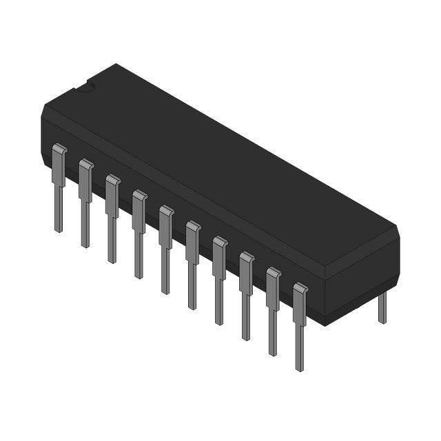
The Texas Instruments CDC204N is a phase-locked loop (PLL)-based clock driver and frequency synthesis device designed for clock distribution and signal conditioning in digital systems requiring low-skew, high-integrity timing signals. It belongs to TI’s early CDC (Clock Driver/Clock Distribution) family, implemented using bipolar or BiCMOS PLL architecture optimized for clock regeneration and fan-out buffering.
## Device Functional Overview and System Role
The CDC204N is designed to take a reference clock input and generate multiple phase-aligned output clock signals with controlled skew and reduced jitter compared to direct fan-out buffering. Its primary system role is clock distribution in synchronous digital systems where multiple subsystems must operate under a common timing reference.
The device integrates a phase-locked loop that locks an internal voltage-controlled oscillator (VCO) to an external reference frequency. Once locked, the PLL ensures that all output clocks maintain a stable phase relationship with the input reference. This architecture enables both frequency multiplication/division (depending on configuration) and regeneration of a clean, low-jitter clock signal from a potentially noisy source.
## PLL Architecture and Frequency Control Mechanism
At the core of the CDC204N is a PLL feedback loop consisting of a phase detector, loop filter, and voltage-controlled oscillator. The phase detector compares the phase of the input reference clock with a divided version of the VCO output. Any phase difference produces an error signal that is filtered and used to adjust the VCO frequency.
The loop filter determines the dynamic response of the PLL, including lock time, jitter attenuation, and stability. The internal VCO generates a clock signal whose frequency is controlled by the filtered phase error voltage. By adjusting the feedback division ratio, the device can generate output clocks that are phase-locked to the input reference but may operate at different frequencies depending on configuration.
This PLL-based regeneration significantly reduces accumulated jitter from the input clock while providing multiple synchronized outputs.
## Clock Distribution and Output Buffering
The CDC204N provides multiple buffered clock outputs derived from the PLL-regenerated internal clock node. Each output is driven by a dedicated output buffer stage designed to maintain consistent rise/fall times and minimize skew between output channels.
Output buffers are designed to drive standard TTL or CMOS-compatible logic loads depending on device implementation. The buffer architecture ensures that all outputs are phase-aligned within a specified skew tolerance, which is critical in systems such as microprocessor buses, memory controllers, and synchronous digital subsystems.
The device emphasizes low output-to-output skew, ensuring deterministic timing relationships across multiple clock domains.
## Input Signal Requirements and Reference Clock Behavior
The reference clock input is designed to accept a stable external clock signal within a defined frequency range specified in the datasheet. The input stage typically includes threshold conditioning circuitry to ensure compatibility with TTL-level or CMOS-level clock sources.
The input signal is used solely as a phase reference and does not directly drive the outputs. Instead, it is used by the phase detector to control the PLL loop dynamics. As a result, the output clock quality is primarily determined by the PLL characteristics rather than the raw input signal quality, although extreme input jitter or instability will still propagate through the system.
## Lock Acquisition and Dynamic Operation
During startup, the PLL enters a lock acquisition phase where the VCO frequency is adjusted until phase alignment with the reference clock is achieved. The lock time is dependent on loop filter characteristics, input frequency stability, and initial frequency offset between the VCO and reference.
Once lock is achieved, the PLL enters steady-state operation, where continuous small corrections are applied to maintain phase alignment. The loop filter suppresses high-frequency jitter components while allowing low-frequency tracking of slow variations in the input clock.
The CDC204N typically includes a lock-detection mechanism or operates with defined behavior during unlock conditions, ensuring that output clocks remain within controlled operating limits during transient conditions.
## Timing Characteristics and Skew Performance
A key performance metric of the CDC204N is output-to-output skew, which defines the maximum timing difference between any two output clock edges. This parameter is critical in synchronous systems where multiple devices must sample data simultaneously.
Propagation delay from input to output is dominated by PLL loop dynamics rather than simple gate propagation delay. This introduces deterministic phase delay but ensures stable frequency relationship across outputs.
The device also exhibits additive jitter characteristics, which are significantly lower than unbuffered fan-out solutions due to PLL-based jitter filtering. Jitter performance is influenced by loop bandwidth and VCO noise characteristics.
## Power Supply and Noise Sensitivity
The CDC204N operates from a regulated supply voltage appropriate for its logic family implementation. Internal PLL and analog circuits are sensitive to power supply noise, making proper decoupling essential for stable operation.
Supply noise can directly modulate VCO frequency, resulting in output jitter degradation. Therefore, power integrity design is a critical aspect of system implementation, particularly in mixed-signal environments where switching noise may be present.
The device typically includes separate supply domains or internal filtering structures to isolate analog PLL circuitry from digital output switching noise.
## Output Electrical Characteristics
Output drivers are designed to provide sufficient current drive capability for standard logic loads while maintaining controlled edge rates. The output stage architecture ensures symmetrical rise and fall times to minimize duty-cycle distortion.
Output voltage levels conform to the logic family requirements defined in the datasheet, ensuring compatibility with downstream digital ICs. The device is intended for direct interfacing with synchronous digital systems without additional level translation in most cases.
Capacitive loading affects output edge rates but does not significantly alter PLL stability, as the PLL operates independently of output loading within specified limits.
## Jitter Performance and Signal Integrity
A primary functional advantage of PLL-based clock distribution is jitter attenuation. The CDC204N reduces high-frequency jitter components present in the input reference through low-pass filtering action of the PLL loop.
Output jitter is determined by a combination of VCO phase noise, loop bandwidth, and internal noise coupling. The device is optimized to maintain low cycle-to-cycle jitter in synchronous systems requiring precise timing alignment.
Signal integrity is further enhanced by uniform output buffering, which ensures consistent waveform characteristics across all outputs.
## Package and Physical Implementation
The CDC204N is provided in a multi-pin package designed for high-density clock distribution applications. The package supports multiple output channels and dedicated power/ground pins to minimize ground bounce and supply noise coupling.
Proper PCB layout is essential to maintain low jitter performance, including controlled impedance routing for clock traces, solid ground planes, and close placement of decoupling capacitors.
The physical design of the package supports high-speed switching operation while minimizing parasitic inductance that could degrade PLL stability or output timing accuracy.
## Application Domains and System Usage
The CDC204N is used in synchronous digital systems requiring distributed clocking, including microprocessor systems, memory subsystems, communication equipment, and industrial control platforms. It is particularly suited for systems where a single reference clock must be distributed to multiple subsystems with minimal skew.
Its PLL-based architecture allows it to regenerate and clean incoming clock signals while providing multiple phase-aligned outputs, making it suitable for timing-critical digital architectures.
## Conclusion
The Texas Instruments CDC204N is a PLL-based clock driver designed for high-precision clock distribution and regeneration. Its architecture combines phase-locked loop frequency synthesis with multi-output buffering to deliver low-skew, low-jitter clock signals across digital systems. The device is optimized for synchronous system timing applications where deterministic clock alignment and signal integrity are critical requirements.