## Overview
The Xilinx XC3SD3400A-4CS484C is a high-capacity FPGA from the Spartan-3A family, featuring System-On-Chip (SoC) capabilities with integrated block RAM and high-speed I/O. It is optimized for cost-sensitive applications requiring moderate logic density, high-speed performance, and low power consumption. The device integrates a large number of logic cells, memory blocks, and configurable I/O for versatile digital design implementation. It is commonly used in embedded systems, data processing, communications, and industrial control applications.
## Core Architecture
* Logic Fabric: Comprises 3-input look-up table (LUT) based configurable logic blocks (CLBs)
* Total logic cells: 342,816 equivalent system gates
* Block RAM: 18 Kb distributed blocks, total 216 Kb
* Digital Signal Processing (DSP) slices: 0 embedded multipliers
* Configurable I/O: Supports LVTTL, LVCMOS, HSTL, and SSTL standards
* High-speed interconnect matrix for deterministic routing between CLBs and I/O
* Global and regional clock management resources with dedicated routing
The architecture provides flexibility for implementing complex combinational and sequential logic while supporting embedded memory and high-speed I/O operations.
## Timing and Performance
* Speed grade: −4 (4 ns typical minimum clock period)
* Maximum user logic clock frequency: up to 250 MHz depending on design
* I/O timing: Input setup and hold times optimized for high-speed interfaces
* Output drive strength configurable per pin
* Glitch-free global clock distribution network
High-speed performance and predictable timing characteristics enable precise synchronous designs and high-throughput signal processing.
## I/O Features
* Total I/O pins: 484
* Programmable slew rate and drive strength
* Supports single-ended and differential signaling
* 3.3 V and 2.5 V I/O banks compatible with various logic standards
* High fan-out capability for driving multiple loads
* Dedicated global I/O pins for clock and reset distribution
The flexible I/O architecture allows interfacing with diverse peripheral devices, memory modules, and communication protocols.
## Memory and Storage
* Distributed RAM in CLBs for small local storage
* 18 Kb block RAM with configurable widths for FIFO, dual-port RAM, or ROM implementations
* Supports synchronous and asynchronous memory access
* Provides on-chip storage for buffering, lookup tables, and temporary computation storage
Embedded memory enables high-performance data handling without external memory dependency.
## Power and Thermal
* Core voltage: 1.2 V typical
* I/O bank voltage: 2.5 V / 3.3 V depending on configuration
* Total power consumption: depends on logic utilization, I/O switching, and clocking, typically 2–5 W for medium-density designs
* Junction temperature range: −40 °C to +85 °C
* Low static and dynamic power design for energy-efficient applications
The Spartan-3A series balances performance and power efficiency, supporting both portable and industrial designs.
## Configuration and Programming
* Configuration method: SelectMAP or JTAG interface
* Non-volatile programming supported via external PROM
* In-system programmability allows design updates without hardware changes
* Bitstream encryption and authentication available for secure designs
* Fast reconfiguration supported with partial reconfiguration techniques
Flexible configuration options facilitate prototyping, design iteration, and field updates.
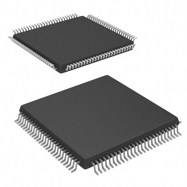
## Package and Mechanical Details
* Package type: CS484 (484-ball Chip Scale Package)
* Ball pitch: 1.0 mm
* Low-profile, compact package suitable for high-density PCB layouts
* RoHS-compliant and lead-free
* Thermal pad for efficient heat dissipation through PCB or heatsink attachment
The package supports high-density placement and thermal management for demanding applications.
## Applications
* Embedded signal processing and control
* Communication and networking equipment
* Industrial automation and motor control
* Consumer electronics with moderate logic density needs
* Data acquisition and real-time processing systems
* Prototyping and educational FPGA platforms
The device is ideal for applications that require a balance between logic capacity, speed, and cost-effectiveness.
## Advantages
* High logic density for complex combinational and sequential designs
* Integrated block RAM for efficient on-chip storage
* Flexible and high-speed I/O for diverse peripheral interfacing
* Fast configuration and partial reconfiguration capability
* Low-power architecture suitable for energy-sensitive applications
* Robust and industrial-grade thermal and voltage tolerance
* Cost-effective FPGA solution for mid-range digital system designs
The Xilinx XC3SD3400A-4CS484C provides a versatile, high-performance, and reliable FPGA platform suitable for embedded systems, communication devices, and industrial control applications requiring moderate to high logic density and integrated memory resources.

.jpg)