Introduction
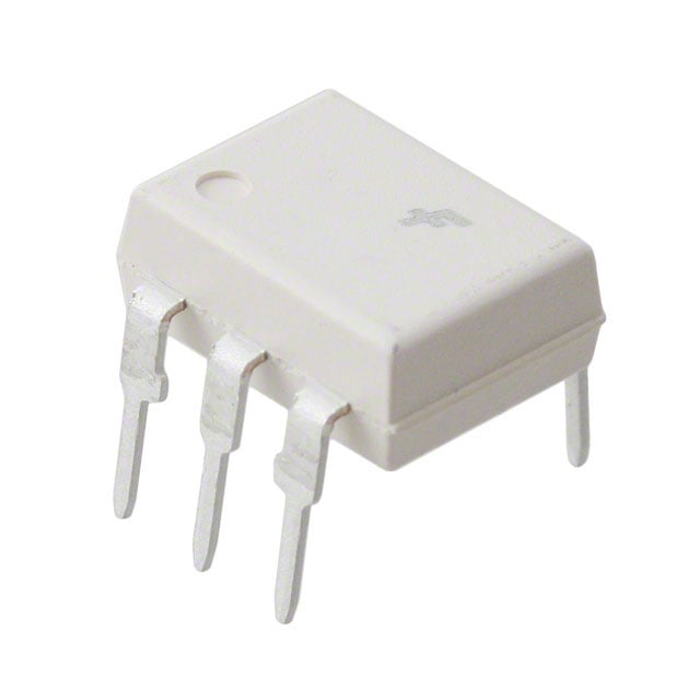
The MCT2ESD is a general purpose phototransistor optocoupler from onsemi, consisting of a gallium arsenide infrared emitting diode optically coupled to a silicon phototransistor with base access. Housed in a compact 6-pin surface-mount device (SMD) package, it provides galvanic isolation between input and output circuits while enabling signal transfer across high voltage barriers. The device supports a wide range of isolation requirements with a rated isolation voltage of 5300 VAC RMS and is designed for reliable operation in both through-hole equivalent and SMD board layouts. Part of the broader MCT2E family, the MCT2ESD variant emphasizes surface-mount compatibility and includes optional white or black package options for different assembly preferences, with Pb-free and RoHS-compliant construction.
Key Features
The MCT2ESD delivers robust isolation performance and flexible interfacing through several core attributes. It achieves a minimum current transfer ratio of 20% at IF = 10 mA and VCE = 10 V, ensuring consistent signal amplification across the isolation barrier. Forward voltage is typically 1.25 V at 20 mA with a maximum of 1.50 V, contributing to low power consumption on the input side. The phototransistor offers a collector-emitter saturation voltage of maximum 0.4 V at IC = 2 mA and IF = 16 mA, along with collector current capability up to 50 mA. Isolation characteristics include 5300 VAC RMS for 1 minute on the primary rating, high isolation resistance of 10^11 Ω minimum, and low isolation capacitance of typically 0.5 pF. The device operates over a wide temperature range of –55 °C to +100 °C, supports UL recognition (File E90700) and optional VDE recognition, and provides base terminal access for external biasing to optimize switching speed or sensitivity. Additional features encompass low dark current of maximum 50 nA and breakdown voltages of 30 V minimum for collector-emitter, 70 V for collector-base, and 7 V for emitter-collector.
Typical Applications
This optocoupler is extensively employed in power supply regulators for feedback isolation, digital logic input protection to separate noisy high-voltage lines from sensitive microcontrollers, and microprocessor interfaces where ground loops must be eliminated. It is also suitable for AC line monitoring, triac driver circuits, telephone line receivers, high-frequency power supply feedback loops, and industrial control systems requiring transient protection. The SMD package variant makes the MCT2ESD particularly advantageous for space-constrained designs in consumer electronics, automotive auxiliary modules, and compact industrial equipment where automated surface-mount assembly is preferred over traditional DIP packages.
Device Architecture
Internally, the MCT2ESD integrates an infrared LED driven by forward current on the input side and an NPN silicon phototransistor on the output side. The optical coupling path ensures high common-mode rejection and isolation without electrical connection. The base pin allows external connection for applications needing faster turn-off times or gain adjustment through base-emitter resistance. The schematic configuration positions the LED anode and cathode on the input and the phototransistor collector, emitter, and base on the output, with one pin typically left as no connection for package standardization.
Pin Configuration and Description
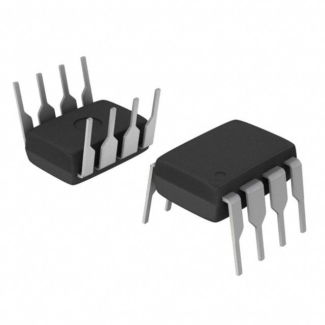
The 6-pin SMD package follows standard optocoupler pinout: pin 1 is the LED anode, pin 2 is the LED cathode, pin 3 is no connection (NC), pin 4 is the phototransistor emitter, pin 5 is the phototransistor collector, and pin 6 is the phototransistor base. This arrangement facilitates straightforward PCB layout with the input and output sides physically separated by the isolation barrier. Pins are formed for surface-mount lead bending, enabling tape-and-reel compatibility and automated placement.
Input Specifications
The emitter (LED) side accepts a maximum continuous forward current of 100 mA (non-M package variant) or 60 mA in certain white package configurations, with a peak pulsed current of 3 A at 300 µs pulse width and 2% duty cycle. Reverse voltage is limited to 3 V, and forward voltage at 20 mA measures typically 1.25 V with a maximum of 1.50 V. Reverse leakage current remains below 10 µA at the rated reverse voltage. Power dissipation on the input side is 150 mW maximum at 25 °C for non-M versions, derating at 2.0 mW/°C above 25 °C. These parameters ensure efficient LED drive while maintaining safe operating margins across the full temperature range.
Output Specifications
The phototransistor detector supports a maximum collector current of 50 mA and collector-emitter voltage of 30 V. Collector-base voltage rating is 70 V, and emitter-collector voltage is 7 V. Saturation voltage between collector and emitter stays at or below 0.4 V under typical drive conditions of IC = 2 mA and IF = 16 mA. Dark current (collector-emitter) is limited to 50 nA maximum at VCE = 10 V and zero LED current, rising to 30 µA maximum over 0–70 °C at lower voltages in some tests. Detector power dissipation is 150 mW at 25 °C with derating of 1.76 mW/°C or higher depending on package variant. Capacitance between collector and emitter is typically 8 pF at zero bias and 1 MHz.
Electrical Characteristics
Under standard test conditions at 25 °C, the current transfer ratio reaches a minimum of 20% when IF = 10 mA and VCE = 10 V (or 5 V in alternative test setups), with no upper limit specified beyond 125% in saturation-related conditions. Collector-emitter breakdown voltage is minimum 30 V (typical 100 V) at IC = 1 mA and zero LED current. Collector-base breakdown is minimum 70 V (typical 120 V) at IC = 10 µA. Emitter-collector and emitter-base breakdowns are each minimum 7 V (typical 10 V). Collector-base dark current stays below 20 nA at VCB = 10 V. These DC parameters guarantee reliable transfer characteristics and minimal leakage, supporting precise signal reproduction across the isolation barrier even at low drive currents.
Switching Characteristics
Switching performance varies with load and bias conditions. In saturated mode with IF = 15 mA, VCC = 5 V, and RL = 2 kΩ (base open), turn-on time is typically 1.1 µs and turn-off time 50 µs. With base resistor of 100 kΩ at IF = 20 mA, turn-on improves to 1.3 µs and turn-off to 20 µs. For non-saturated operation typical of white package variants or specific tests (IF = 10 mA, VCC = 10 V, RL = 100 Ω), both turn-on and turn-off times are approximately 2 µs. Rise and fall times align closely with these delay figures, enabling the device for medium-speed digital isolation up to several hundred kHz depending on circuit configuration and external components.
Isolation and Safety Ratings
The MCT2ESD provides input-to-output isolation voltage of 5300 VAC RMS for 1 minute on the standard black package rating (with higher peak values of 7500 V for 1 second in white package options). Isolation resistance exceeds 10^11 Ω at 500 VDC, while isolation capacitance remains low at typically 0.5 pF (0.2–2 pF range in white variants). Safety approvals include UL recognition and optional VDE certification for reinforced insulation in applicable mains voltage classes. Creepage and clearance distances meet industry standards for the SMD footprint, and the device is rated for pollution degree 2 environments with appropriate external protection.
Thermal and Power Derating
Total device power dissipation is 250 mW at 25 °C for standard packages, with linear derating of approximately 2.94–3.3 mW/°C above 25 °C depending on exact variant. Operating ambient temperature spans –55 °C to +100 °C, and storage extends to +150 °C. Lead soldering is supported up to 260 °C for 10 seconds. These thermal limits ensure long-term reliability when proper PCB heat sinking and airflow are considered in high-density SMD layouts.
Package Information
The MCT2ESD utilizes a 6-pin SMD package with body dimensions approximately 8.89 mm × 7.62 mm and standard lead pitch of 2.54 mm. Leads are formed for surface mounting with minimum lead length and seating plane optimized for automated reflow processes. The package supports both tape-and-reel and tube delivery formats and is fully compatible with standard SMT assembly lines. Marking includes the device code and date codes for traceability.
Ordering and Customization Details
The part number MCT2ESD designates the surface-mount version of the MCT2E family optocoupler with the specified isolation and phototransistor base access. It is supplied in Pb-free, RoHS-compliant form and is optimized for high-volume production. Equivalent family members allow selection between DIP and additional SMD configurations or enhanced CTR variants without altering the fundamental electrical performance. The device meets all specified parameters across its industrial temperature grade and is ideal for designs transitioning from legacy through-hole to modern surface-mount technology.