General Description
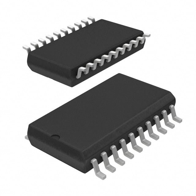
The L4971D is a step-down monolithic power switching regulator from STMicroelectronics capable of delivering up to 1.5A of continuous output current at a regulated voltage adjustable between 3.3V and 50V. Fabricated using BCD mixed technology, it integrates an internal power DMOS transistor with a typical RDS(on) of 0.25Ω, enabling high efficiency and fast switching speeds. The device supports a wide input voltage range from 8V to 55V and achieves switching frequencies up to 300kHz, provided package power dissipation limits are respected. Output voltage is set by a simple external resistive divider, with a precise internal 3.3V reference accurate to ±1%. Key protection and control features include pulse-by-pulse current limiting, hiccup-mode short-circuit protection, voltage feedforward for improved line regulation, soft-start to limit inrush current, protection against feedback loop disconnection, an inhibit pin for zero-current shutdown, and thermal shutdown. The L4971D variant is specifically packaged in a wide SO16W surface-mount outline, optimized for automated SMD assembly while maintaining the same electrical performance as the DIP8 version of the L4971 family.
Key Features
The L4971D offers a comprehensive set of advanced capabilities tailored for efficient DC-DC conversion. It provides up to 1.5A step-down conversion with an operating input voltage spanning 8V to 55V. The internal reference voltage is precisely 3.3V with ±1% tolerance. Output voltage is fully adjustable from 3.3V to 50V via an external divider. Switching frequency is user-adjustable up to 300kHz through external resistor and capacitor on the oscillator pin, with automatic line feedforward compensation. The regulator supports zero-load current operation and incorporates internal current limiting with both pulse-by-pulse and hiccup-mode protection for robust short-circuit handling. An inhibit function enables zero current consumption in standby. Additional safeguards include dedicated protection against feedback disconnection and integrated thermal shutdown. A soft-start function is implemented via an external capacitor on the SS/INH pin. The internal DMOS switch and voltage feedforward ensure high efficiency and stable regulation across the full input range.
Applications
The L4971D is well-suited for a broad range of general-purpose step-down power supply designs requiring high efficiency, wide input voltage tolerance, and adjustable output up to 1.5A. Typical uses include industrial and consumer electronics power modules, battery chargers, LED drivers in series configurations, distributed power systems in telecom or automotive auxiliary supplies, and any application needing a compact, high-voltage capable buck converter. Its ability to operate from 8V to 55V inputs makes it ideal for systems powered by 12V, 24V, or 48V rails, while the adjustable output down to 3.3V supports modern logic and analog loads. The surface-mount SO16W package facilitates dense PCB layouts in space-constrained equipment such as instrumentation, point-of-load regulators, and portable industrial tools.
Pin Configuration
The L4971D in SO16W package features the following pinout (with equivalent DIP8 references for clarity):
Pin 1 (NC), Pin 2 (GND – ground), Pin 3 (SS_INH – soft-start/inhibit input: logic low disables the device and controls soft-start timing via external capacitor), Pin 4 (OSC – oscillator pin: external resistor to VIN and capacitor to ground set frequency with automatic feedforward), Pins 5 and 6 (OUT – step-down regulator output), Pin 7 (NC), Pin 8 (NC), Pin 9 (NC), Pin 10 (NC), Pin 11 (VCC – unregulated DC input voltage), Pin 12 (BOOT – bootstrap capacitor connection to OUT for internal DMOS gate drive), Pin 13 (COMP – error amplifier output for external frequency compensation), Pin 14 (FB – feedback input: direct connection yields 3.3V output; external divider required for higher voltages), Pin 15 (NC), Pin 16 (NC).
Unused pins in the SO16W are not internally connected to the die. The inhibit pin accepts an open-collector or open-drain drive for shutdown.
Absolute Maximum Ratings
Key absolute maximum ratings include: input voltage (VCC) up to 58V; output DC voltage down to -1V with peak transient to -5V at 200kHz; bootstrap voltage (BOOT to OUT) up to 70V; maximum internal limiting output current 14A peak; analog input voltages limited to 12V or 13V depending on pin and VCC level; power dissipation at Tamb ≤ 60°C is 0.8W for the SO16W package; junction and storage temperature range from -40°C to 150°C. These ratings ensure safe operation within specified thermal and electrical boundaries.
Thermal Data
Thermal resistance junction-to-ambient (Rth(j-amb)) for the SO16W package is 110°C/W when mounted on a standard PCB. This value must be considered when calculating maximum allowable power dissipation to prevent thermal shutdown activation at junction temperatures approaching 150°C.
Electrical Specifications
Under recommended conditions (Tj = 25°C, Cosc = 2.7nF, Rosc = 20kΩ, VCC = 24V unless otherwise noted, with specifications extended to Tj = 0°C to 125°C), the L4971D exhibits the following performance:
Operating input voltage range is 8V to 55V for output voltages from 3.3V to 50V at 1.5A load. Fixed 3.3V output measures 3.33V min to 3.39V max at 0.5A, with line regulation maintaining 3.22V min to 3.5V max across full input range. Dropout voltage is typically 0.44V (max 0.55V) at VCC = 10V and 1.5A, increasing under higher temperature. Maximum limiting current is 2A min to 3A max. Efficiency reaches 85% typical at 3.3V output and 1.5A load. Switching frequency is 90kHz min to 110kHz max under nominal conditions, with line stability of 3% to 6% and temperature stability up to 4%. Supply voltage ripple rejection is 60dB typical at 100Hz.
Soft-start charge current is 30µA to 50µA typical 40µA, with discharge current 6µA to 14µA. Inhibit low-level voltage threshold is 0.9V max, with source current 5µA to 15µA. Total operating quiescent current is 4mA to 6mA, quiescent current at zero duty cycle and VFB = 3.8V is 2.5mA to 3.5mA, and standby quiescent current drops to 100µA to 200µA (up to 150µA–300µA at VCC = 55V) when inhibited.
The error amplifier provides a feedback voltage of 3.33V to 3.39V, line regulation of 5mV to 10mV across 8V–55V, reference temperature stability of 0.4mV/°C typical, high-level output voltage 10.3V min, low-level 0.65V max, source/sink output currents 200µA to 300µA, bias current 2µA to 3µA, supply ripple rejection 60dB to 80dB, open-loop gain 50dB to 57dB, and transconductance 2.5mS.
Oscillator section parameters include ramp valley voltage 0.78V to 0.92V, ramp peak 2V to 2.3V at VCC = 8V or 9V to 10.2V at VCC = 55V, maximum duty cycle 95% to 97%, and maximum frequency up to 300kHz with Rosc = 13kΩ and Cosc = 820pF at zero duty cycle. These characteristics guarantee precise PWM control and stable operation across temperature and line variations.
Functional Overview
The L4971D operates as a voltage-mode controlled buck converter with an internal DMOS power switch. The oscillator section generates a ramp signal whose frequency is set externally, automatically incorporating voltage feedforward for constant frequency and improved transient response. The PWM comparator modulates the duty cycle by comparing the error amplifier output to the oscillator ramp. The error amplifier regulates the output via the FB pin, supporting direct 3.3V operation or higher voltages with a divider. Pulse-by-pulse current limiting monitors switch current, while persistent faults trigger hiccup-mode protection. Soft-start ramps the reference gradually via the SS/INH pin capacitor to avoid output overshoot. The inhibit pin forces zero-current sleep mode when pulled low. Feedback disconnection protection prevents uncontrolled output rise. Thermal shutdown activates if junction temperature exceeds safe limits. An external bootstrap capacitor ensures proper gate drive for the high-side DMOS. Minimal external components are required: input/output capacitors, inductor, freewheeling diode, oscillator RC, compensation network, and soft-start capacitor. Typical application circuits achieve high efficiency with inductors around 126µH and capacitors sized for ripple control, using Schottky diodes such as STPS3L60U for low forward drop.
Package Information and Ordering
The L4971D is housed in a wide-body SO16W surface-mount package with dimensions: A (2.35mm to 2.65mm), D (10.10mm to 10.50mm), E (7.40mm to 7.60mm), e (1.27mm), H (10.0mm to 10.65mm), and lead pitch compliant with standard SMD processes. Mold flash limits are 0.15mm maximum per side. This package supports automated assembly and offers 0.8W power dissipation capability. Ordering is under the code L4971D for the SO16W variant in tube or tape-and-reel formats, covering the full -40°C to 150°C junction temperature range. The design minimizes board space while delivering the full 1.5A capability with appropriate heatsinking via copper planes.