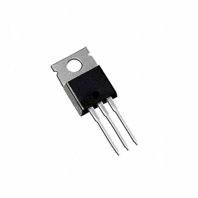
Infineon Technologies IRF100S201 is a discrete N-channel power MOSFET belonging to the StrongIRFET™ family developed for high-current power conversion and motor-control applications. The device is designed for low conduction loss, high continuous drain current capability, and robust operation in demanding switching environments. It is implemented using advanced power MOSFET technology optimized for low drain-to-source on-resistance and efficient thermal performance within a surface-mount D2PAK package structure. The component is intended primarily for power switching applications rather than linear amplification and is widely used in industrial power systems, DC motor drives, synchronous conversion stages, and high-current switching architectures.
## Device Classification and Functional Positioning
The IRF100S201 is classified as an enhancement-mode N-channel power MOSFET. In enhancement-mode operation, the transistor remains normally off until a sufficient positive gate-to-source voltage is applied. Once the gate voltage exceeds the threshold region, a conductive channel forms between drain and source terminals, allowing current flow controlled by the gate-drive level.
The device is optimized for applications requiring low static conduction loss and strong ruggedness characteristics. Compared with bipolar power transistors, the MOSFET structure eliminates minority-carrier storage effects, enabling faster switching behavior and simpler gate-drive implementation. The StrongIRFET™ family emphasizes robustness under inductive switching conditions and reliable operation under high-current stress environments.
Internally, the device includes an intrinsic body diode formed by the MOSFET semiconductor structure. This diode supports reverse-current conduction in bridge-based switching topologies and inductive load systems, although its reverse recovery behavior must still be considered in high-frequency switching applications.
## Electrical Characteristics
The IRF100S201 is designed for medium-voltage power systems and supports substantial continuous drain current capability under controlled thermal conditions. One of its primary electrical characteristics is low drain-to-source on-resistance when driven with an appropriate gate voltage. Low RDS(on) minimizes conduction losses and improves overall conversion efficiency in high-current systems.
The transistor is intended for operation with conventional power MOSFET gate-drive amplitudes rather than direct low-voltage logic drive. Adequate gate voltage is required to fully enhance the channel and achieve the specified low-resistance operating region. Insufficient gate drive may increase conduction loss and thermal dissipation.
The device exhibits relatively high gate charge because of its large silicon die area and current capability. Total gate charge directly influences switching speed and gate-driver power requirements. In practical designs, the gate-driver circuit must provide sufficient peak current capability to rapidly charge and discharge the MOSFET input capacitances during switching transitions.
Power dissipation capability is strongly dependent on package thermal conditions and PCB implementation. Thermal resistance between the semiconductor junction and external mounting structure is optimized for efficient heat transfer into copper planes or heatsinks.
## Switching Characteristics and Dynamic Performance
The IRF100S201 is intended primarily for low-frequency and moderate-frequency hard-switching applications. Although capable of relatively fast switching compared with bipolar technologies, the device is optimized more for current capability and ruggedness than ultra-high-frequency switching efficiency.
The MOS gate structure behaves as a capacitive input network consisting primarily of gate-source and gate-drain capacitances. During switching events, the gate driver must overcome the Miller capacitance region, which influences switching transition timing and switching loss characteristics.
Switching performance depends heavily on external circuit conditions including gate resistance, PCB parasitic inductance, supply decoupling quality, and load current magnitude. Poor layout practices may generate voltage overshoot, ringing, or excessive electromagnetic interference during high di/dt switching events.
The intrinsic body diode provides a reverse-current conduction path in synchronous rectification and bridge topologies. However, reverse recovery current and associated switching losses must be evaluated carefully in high-speed switching systems where commutation efficiency is critical.
## Operating Conditions and Design Constraints
Reliable operation of the IRF100S201 requires maintaining junction temperature, gate-source voltage, and drain current within specified limits. Thermal management is particularly important because conduction and switching losses can become substantial at high load current levels.
The D2PAK package supports effective thermal coupling to PCB copper structures and external cooling systems. Proper solder attachment and sufficient copper area are necessary to achieve intended thermal performance. Inadequate thermal design may increase junction temperature and reduce long-term reliability.
The gate oxide structure is sensitive to excessive voltage stress. Designers must ensure that gate-source voltage remains within the allowable operating range under both steady-state and transient conditions. Gate protection techniques may be required in electrically noisy environments.
Because the package tab is electrically connected to the drain terminal, layout and heatsink isolation strategy require careful consideration. Improper grounding or insufficient isolation may create unintended electrical coupling paths in multi-device power assemblies.
High-current switching loops should be minimized to reduce parasitic inductance and transient voltage spikes. Decoupling capacitors should be placed close to the switching stage to stabilize the supply network during rapid current transitions.
## Input and Output Characteristics
The gate terminal exhibits extremely high DC input impedance because of the insulated MOS structure. Steady-state gate current is therefore negligible, although transient charging current during switching can be significant because of the device capacitances.
When fully enhanced, the drain-source conduction path behaves approximately as a low-value resistive channel. Conduction loss increases proportionally with the square of drain current and is also temperature dependent because channel resistance rises with junction temperature.
The source terminal acts as both the gate-drive reference and current return path. Excessive source inductance may degrade switching behavior and introduce gate-drive instability, particularly in high-current or fast-switching applications.
Avalanche ruggedness is an important characteristic of the StrongIRFET™ family. The device is designed to tolerate controlled inductive switching stress within specified limits, improving survivability in motor-drive and inductive-load environments.
## Typical Application Areas
The IRF100S201 is commonly used in brushed DC motor controllers, industrial power converters, synchronous rectification stages, battery-powered switching systems, inverter modules, and high-current DC distribution architectures.
In motor-control systems, the device is suitable for half-bridge and full-bridge switching structures requiring high pulsed-current capability and efficient conduction performance. In DC-DC converter applications, it may operate as a primary switching transistor or synchronous rectifier depending on converter topology.
Battery-management and power-distribution systems benefit from the low conduction loss and strong thermal capability of the device, especially in applications involving repetitive transient current demand and continuous-duty operation.
## Conclusion
Infineon Technologies IRF100S201 is a rugged medium-voltage N-channel StrongIRFET™ power MOSFET optimized for high-current switching applications. The device combines low drain-to-source on-resistance, substantial current-handling capability, strong avalanche ruggedness, and efficient thermal performance within a D2PAK package architecture. Successful implementation requires proper gate-drive design, controlled PCB parasitics, effective thermal management, and careful handling of switching transients. Within its intended operating conditions, the IRF100S201 provides reliable and efficient performance for industrial power conversion, motor control, and high-current switching systems.